The complexity of printed circuit board assembly (PCBA) is growing and so is the need for testing to ensure quality, reliability and functionality on the electronic manufacturing floor.
As we continue to push the boundaries of what’s possible with electronics, the demand for reliable and high-performing electronic systems continues to grow. As a result, the complexity of printed circuit board assembly (PCBA) is growing and so is the need for testing to ensure quality, reliability and functionality on the electronic manufacturing floor.
Challenge #1: Increasing PCBA density and high-volume demand in manufacturing
As technological progress moves forward, there’s been a significant change in the desire for compact and intricately designed devices. This has sparked significant evolution in PCBA design, characterized by two key developments:
Device miniaturization, in response to the growing demand for everything smaller and faster. As a result, designers are actively increasing the functionality of the PCBA, thereby increasing the number of components that require test access.
There is a high volume of PCBA, and while the increase in test access is inevitable, this volume growth has created a bottleneck in in-circuit test (ICT) systems.
Addressing these challenges means leveraging technology that can accommodate more test nodes. This ultimately means increasing the capacity and allowing for processing larger panels.
Challenge #2: Longer short test on high-impedance node
A short test is a standard unpowered test conducted during ICT. This test checks for unwanted shorts between components on a PCBA. The short test also helps to protect the board from damage in the subsequent powered tests phase. As technology evolves, the prevalence of high-impedance nodes has been increasing, driven by the growing demand for signal quality, lower power consumption and improved functionality.
However, short test duration for the high-impedance node is notably longer. On average, it takes three times as long to test a high-impedance node compared to a low-impedance node. This discrepancy in testing arises due to the unique characteristics of high-impedance nodes, which require longer stabilization time due to the low current flow, and how small amounts of noise can affect measurements. Therefore, testers must apply the test signal for an extended period to stabilize the voltage or current to ensure accurate readings. There is also complexity during short isolation when a short is detected on a high-impedance node, isolating and identifying the specific shorted nodes can be a more complex process. This extended testing time could potentially impede the overall test throughput of the manufacturing line, posing challenges to efficiency and production speed.
Addressing the challenges associated with testing high-impedance nodes, the enhanced short test comprises of two phases: a detection phase and an isolation phase. Specifically designed to enhance the efficiency of short detection for high-impedance nodes, this new algorithm is not applicable to low-impedance nodes or nodes with known shorts.
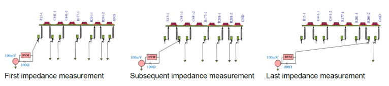
Figure 1: High-impedance nodes are broken down into groups using the binary ID and measured for resistance to check for shorts.
Consider a scenario where a board contains 100 high-impedance nodes. In this case, each node will have a 7-bit identifier length. Through the implementation of the enhanced short test, the testing process was significantly streamlined, requiring only seven iterations to complete the test instead of 100. Consequently, this reduction in the number of iterations effectively minimizes the overall test duration.
During the isolation phase, if a short circuit is detected, the enhanced short test method employs the halving technique to pinpoint the specific nodes where the unexpected short has occurred, mirroring the standard algorithm. However, a key distinction lies in the sequence: The shorted nodes are initially identified from one group and subsequently from the other, optimizing the efficiency of the identification process.
Challenges #3: Testing supercapacitors (1 to 100 Farads) in in-circuit testing
Supercapacitors, often referred to as SuperCaps, are a type of capacitors characterized by their high capacitance, ranging from 1 farad to 100 farads. Capacitors, in general, are electrochemical devices designed to store energy in the form of electrostatic energy.
The exceptional energy storage capacity of supercapacitors makes them particularly valuable in a number of applications, such as supporting electric and hybrid vehicles (EVs/HEVs) and plug-in hybrid electric vehicles (PHEVs). They are utilized for stop-start functionality, rapid acceleration and regenerative braking operations.
In addition to their automotive applications, supercapacitors serve as a secondary power source, providing emergency backup power to critical systems in the event of a failure or during startup procedures. Moreover, they play a crucial role in maintaining stable voltage levels within a vehicle’s electrical system, thereby enhancing power quality. This stability ensures that sensitive electronic components receive a consistent and reliable power supply, contributing to overall system reliability and performance.
It is therefore essential to charge, test and discharge supercapacitors with precision.

Figure 2: SuperCap test connection
Challenge #4: Low current measurements in in-circuit testing
The leakage and sleep currents play a crucial role in the performance of various devices, including mobile devices, medical equipment and automotive units. These currents are particularly significant indicators of a device’s energy consumption, providing insights into how long the battery can sustain operation before requiring recharging or replacement.
In automotive applications, engine control units (ECUs) exemplify the importance of managing leakage and sleep currents. ECUs oversee critical functions within an engine’s operation, such as climate control, airbag management and anti-lock braking systems. Inefficient handling of these currents within ECUs can result in an unnecessary drain on the battery, leading to shortened battery life and potential electrical malfunctions.
Beyond efficiency concerns, leakage currents also pose a significant safety risk. Malfunctions induced by these currents may cause safety-critical circuits within ECUs to behave unpredictably, potentially resulting in hazardous situations. For instance, malfunctioning safety systems could lead to the failure to deploy airbags during a collision. Considering these potential risks, meticulous low-current measurements are imperative.
Challenge #5: Limited test access on PCBA
Achieving comprehensive testing of a high-density PCBA requires test points to be positioned on every electrical node throughout the circuit, allowing the in-circuit tester to perform thorough component and connection tests. However, accommodating test points on all electrical nodes within a densely packed PCBA is impractical. This limitation in test point allocation leads to a decrease in test coverage for a high-density PCBA.
This can be addressed by introducing automated cluster formation and test generation for these clusters. An automated feature computes the equivalent impedance of the passive analog cluster and compares it with measurement results. Subsequently, creating a comprehensive test plan tailored for measuring cluster components on densely packed PCBAs. This significantly reduces the engineering effort required to manually identify clusters and generate tests.

Figure 3: Types of devices and which devices are accepted for cluster test.
The enhanced cluster test algorithm is introduced in the high-density in-circuit tester and presents an automated solution for creating dependable passive device clusters and generating test plans. Leveraging the power of an algorithm from the advanced cluster library (ACL) ensures efficient cluster formation. Subsequent stages involve stringent hardware requirement validation, contributing to identifying reliable clusters for testing purposes. By streamlining the process, even novice test engineers can effectively execute tests. This advancement holds the potential for customers to enjoy improved testing precision, quicker test execution and enhanced reliability in their production processes, all facilitated by the automated cluster test algorithm.
Summary
To address today’s PCBA test challenges, it is essential to reduce the number of iterations, consequently decreasing the testing duration required for high-density PCBAs. By enabling faster test times and reimagining test coverage, manufacturers will be able to overcome the complexities.
Source from: EE Times


